
System Overview
System-Level Block Diagram
The system-level block diagram is shown in Fig.1. The chip contains five modules: a low-noise amplifier (LNA), a mixer, a differential-to-single converter, a limiting amplifier, and a digital demodulator. Radio-frequency (RF) signals are first picked up by the antenna. Then out-of-band signals are filtered out by an off-chip band-selection filter. Only the desired signals in the FM band are left. Next the signals flow into the LNA to get amplified. The desired signal is converted down to baseband by the mixer, and converted from differential to single-ended. Finally, the limiting amplifier converts the baseband signal to a logic waveform, which is demodulated by the digital FM demodulator. The clock signals for the mixer and the digital FM demodulator are generated off chip.
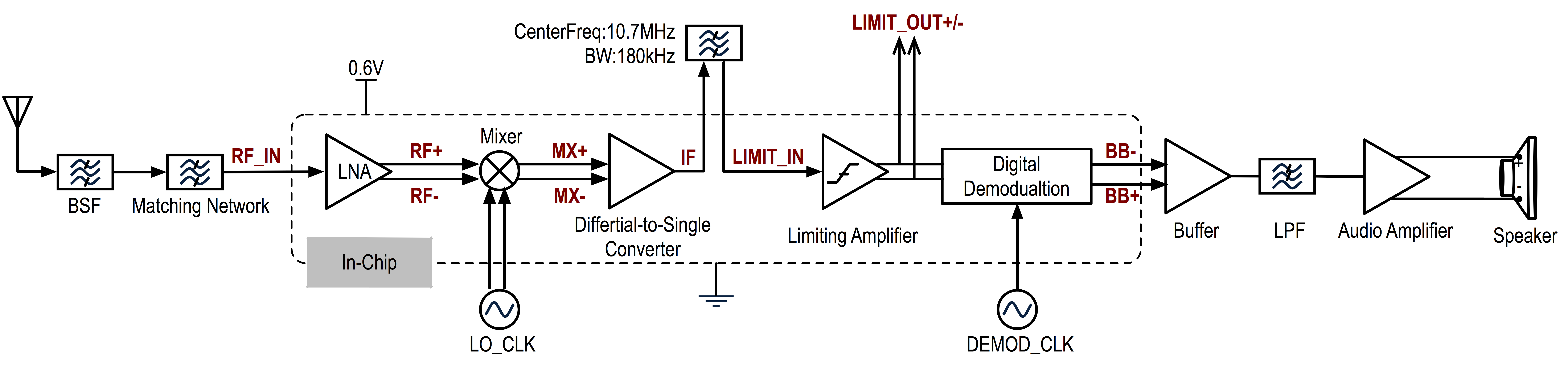
Fig.1 System-Level Simplifed Block Diagram
Pinout and Package Definition
A QFN-28 SMD package has been used in this project to reduce parasitics associated with bond wires and packages. The top view of the QFN-28 pinout diagram is shown in Fig.2. Pin definitions are in Tab.1.
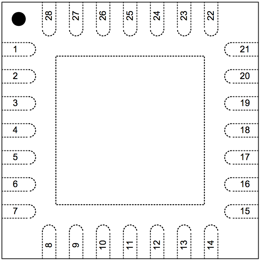
Fig.2 QFN-28 Pinout Diagram
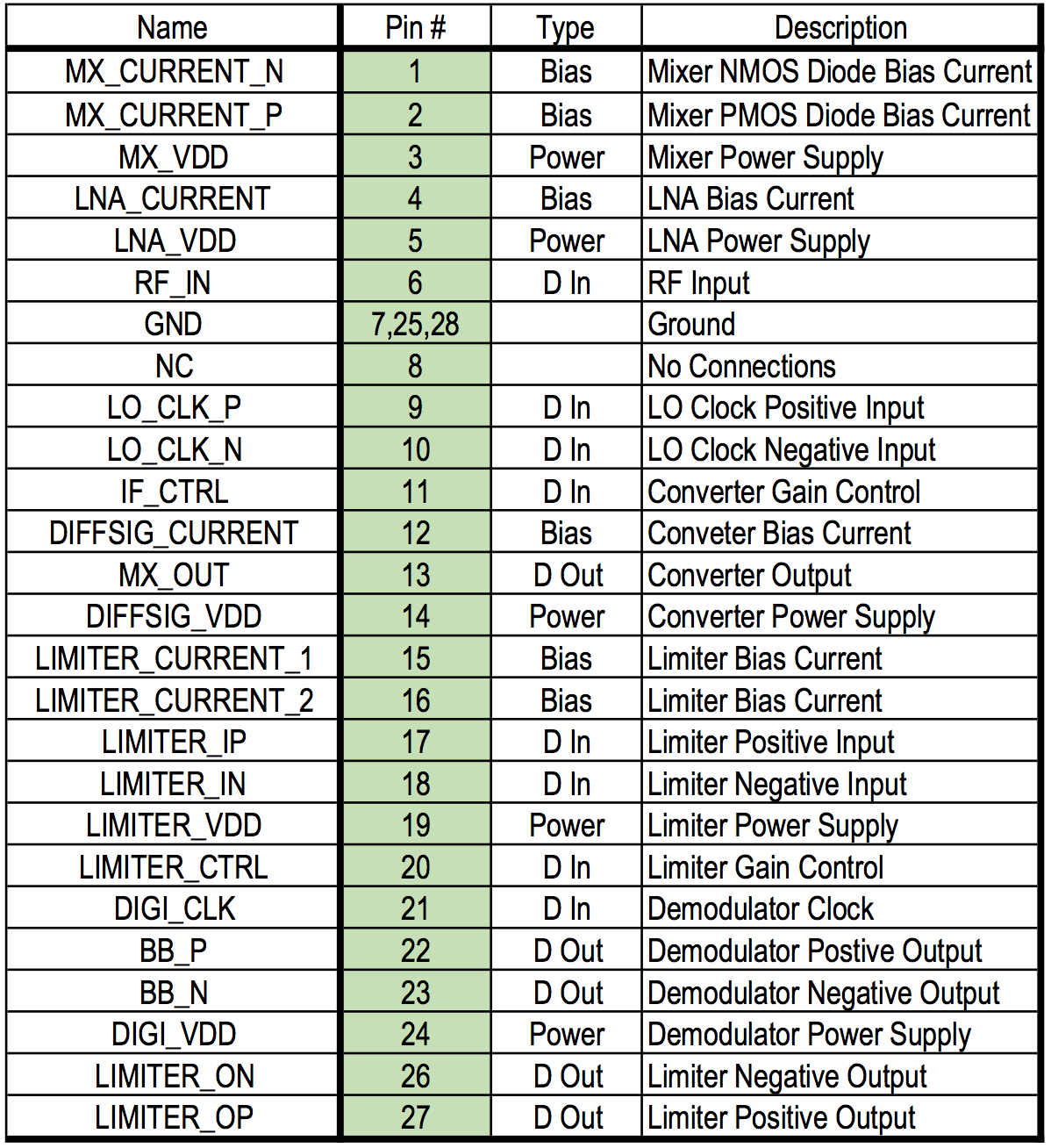
Tab.1 Pin Definitions